Short answer: LED chip reliability testing combines baseline optical and electrical measurements, controlled stress tests, periodic remeasurement, and failure analysis. A useful program checks luminous-flux maintenance, forward voltage, reverse leakage, color stability, thermal behavior, wire bonds, die attachment, and package integrity. The exact stress level and pass/fail limits must come from the LED datasheet, the intended application, and the applicable test standard.
This guide explains a practical LED quality testing workflow for bare chips, packaged LEDs, and LED display components. It also shows how to separate chip degradation from failures caused by packaging, bonding, heat, moisture, or the test fixture.
What Does LED Chip Reliability Testing Measure?
Reliability testing estimates whether an LED will continue to meet its specified performance under expected electrical, thermal, mechanical, and environmental stress. It is not a single test and it does not prove an exact service life. Instead, it produces evidence about degradation rate, failure modes, process consistency, and manufacturing risk.
The most useful parameters are:
- Optical: luminous flux or radiant flux, intensity, wavelength or color coordinates, and color shift.
- Electrical: forward voltage (Vf), reverse leakage, operating current, and open- or short-circuit failures.
- Thermal: junction-temperature behavior, thermal resistance, heat dissipation, and temperature rise.
- Mechanical: wire-bond pull strength, die shear strength, solder-joint integrity, and package cracking.
- Visual: dark spots, delamination, corrosion, resin yellowing, bond damage, and contamination.
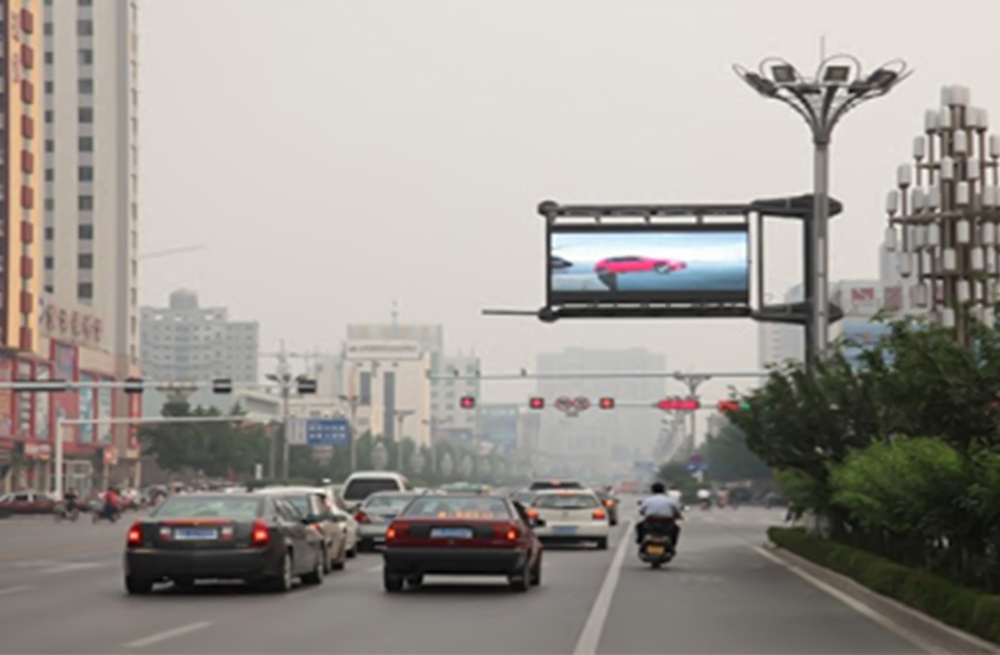
For LED sign and display applications, the goal is broader than testing the die alone. LED chip packaging testing, PCB reliability testing, power stability, and thermal management can all affect brightness uniformity and field life.
Recommended LED Reliability Test Matrix
| Test | What it reveals | Typical measurements |
|---|---|---|
| Initial optical and electrical test | Baseline performance and outliers | Flux, Vf, leakage, wavelength, color coordinates |
| Operating life test | Light-output degradation and electrical drift under power | Flux maintenance, Vf shift, failures over time |
| High-temperature storage | Material and contact stability without electrical load | Visual defects, leakage, Vf, optical change |
| Temperature cycling or thermal shock | Damage caused by expansion mismatch and repeated temperature change | Cracks, delamination, bond and solder failures |
| Damp heat / high humidity | Moisture sensitivity, corrosion, and package sealing weakness | Leakage, corrosion, optical loss, visual defects |
| LED chip shear-force test | Strength of the die attach | Peak shear force and failure location |
| LED chip pull-force or wire-bond pull test | Bond-wire and interconnect quality | Peak pull force and failure mode |
| Final inspection and failure analysis | Root cause and whether failure is chip-, package-, or process-related | Microscopy, electrical tracing, cross-section when needed |
Use standards that match the product and customer requirement. IEC 60068 and JEDEC JESD22 families contain widely used environmental and mechanical methods. IES LM-80 addresses lumen maintenance for LED packages, arrays, and modules; it should not be treated as a complete bare-chip qualification standard.
How to Test LED Chip Reliability: Step by Step
1. Define the use case and failure criteria
Start with the real operating environment: current, duty cycle, expected junction temperature, humidity, vibration, outdoor exposure, and required service life. Then define failure before testing begins. Examples include an open circuit, excessive reverse leakage, a specified drop in luminous flux, unacceptable color shift, or a mechanical strength value below the approved limit.
There is no universal pass/fail number for every LED. Record the device part number, package type, lot, datasheet rating, acceptance limit, equipment, calibration status, and measurement uncertainty in the test plan.
2. Build a representative sampling plan
Reliability is normally evaluated by sampling, so sample selection directly affects the conclusion. Random sampling from a single convenient location can miss wafer-level variation. Divide the wafer or production lot into zones and take samples from each zone. Keep lot identity and sample position traceable.
An illustrative legacy plan for small chips below approximately 0.3 x 0.3 mm used 8 to 10 samples distributed across four wafer zones. When results were inconsistent, the sample size increased to 16 to 20 devices. These numbers are examples, not universal requirements; a formal plan should be based on risk, lot size, expected failure rate, and the confidence level required.
3. Record baseline optical and electrical data
Stabilize the devices at the specified temperature, drive them with a calibrated constant-current source, and measure every sample before stress begins. Use the same fixture geometry and, where possible, the same calibrated equipment and operator for baseline and final measurements.
For optical comparison, total luminous flux or a controlled integrating-sphere measurement is generally more repeatable than a single axial-intensity reading. Narrow viewing angles can make intensity readings highly sensitive to small positioning changes.
4. Apply controlled life-test stress
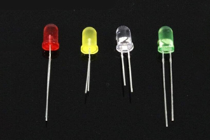
Operating life tests may use rated conditions or an approved accelerated condition. One historical example used 30 mA at 25 +/- 5 degrees C with checkpoints at 96, 1,000, and 5,000 hours for low-power packaged samples. The 30 mA condition represented about 1.5 times the rated current in that specific case.
Do not reuse this condition without checking the current device rating and junction temperature. Excessive current can create a different failure mechanism from the one seen in normal use, which makes the life estimate misleading. Monitor current, ambient temperature, fixture temperature, and interruptions throughout the test.
5. Add packaging and mechanical checks
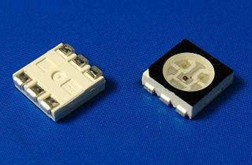
Bare dies and packaged LEDs should not be interpreted in the same way. A bare chip normally dissipates heat more directly and is not exposed to bond-wire, resin, and package-interface failure modes. A packaged-device test better represents actual use, but the result includes both chip and package reliability.
For LED packaging reliability evaluation, inspect die attach, wire bonding, encapsulant, lead frame, and solder interfaces. A die-shear test checks die-attach strength; a wire-bond pull test checks interconnect strength. The peak force alone is not enough. Record where the sample failed, because a wire break, bond lift, die fracture, and adhesive failure point to different process problems.
Use the approved fixture, tool geometry, loading direction, and test speed for the package. Acceptance thresholds should be specified by the manufacturer, customer, or applicable standard rather than copied from an unrelated LED type.
6. Control package aging and environmental effects
Epoxy and other encapsulants can yellow or lose transparency after prolonged ultraviolet, heat, and oxygen exposure. Moisture can increase leakage or corrosion, while thermal cycling can stress materials with different expansion coefficients. These effects may reduce measured light output even when the semiconductor die remains functional.
Protect control samples from unintended UV exposure, keep unstressed reference devices, and document preconditioning. If a long-term test shows optical loss, compare electrical drift and package appearance before assigning the failure to the chip.
7. Remeasure at planned checkpoints
At every checkpoint, use the original measurement conditions. Allow samples to stabilize before reading them, and avoid changing the fixture, optical distance, instrument settings, or ambient conditions. Calculate both the individual change and the lot distribution; an average can hide a small group of early failures.
Useful outputs include:
- Flux maintenance: final flux divided by initial flux, expressed as a percentage.
- Change in forward voltage and reverse leakage.
- Color-coordinate or dominant-wavelength shift.
- Number, time, and type of catastrophic failures.
- Mechanical-test value and the observed failure mode.
- Mean, spread, minimum, maximum, and outliers for each checkpoint.
How to Design a Stable LED Life-Test Bench
A life-test bench needs a regulated constant-current source, safe power distribution, temperature monitoring, sample identification, timing or data logging, and protection against a single failure disrupting the entire test. The original bench shown below used modular boards and multiple DC channels to test many LED groups at once.
Parallel-connected LEDs can share current unevenly because forward voltage decreases as temperature rises. A warmer LED may draw more current, become hotter, and distort the comparison. Individual regulated channels are preferable. When a series string is used, every LED carries the same current, but an open device can turn off the entire string. Design monitoring so the failed sample and failure time can still be identified.
Before a long run, verify channel current under load, polarity, connector resistance, airflow, data logging, over-temperature protection, and recovery after a power interruption. Keep the test bench within its rated electrical and thermal capacity.
How to Interpret LED Reliability Test Results
A reliable conclusion connects the measured change to a failure mechanism. If light output falls while Vf and leakage remain stable, inspect the encapsulant, optical surface, and measurement geometry. If leakage rises after humidity stress, examine contamination, corrosion, and package sealing. If failures cluster in one wafer zone or production lot, investigate process uniformity. If a bond test fails at the interface rather than in the wire, review bonding energy, force, temperature, and surface condition.
Do not use accelerated test hours as service-life hours through a simple one-to-one conversion. Lifetime projection requires a justified acceleration model, multiple stress levels, adequate sample size, and evidence that the accelerated stress did not introduce a new failure mode.
LED Quality Testing Checklist
- Define the application, rated conditions, stress profile, and pass/fail limits.
- Use traceable samples from representative wafer zones or production lots.
- Calibrate the current source, optical instruments, temperature sensors, and mechanical tester.
- Measure and save baseline optical, electrical, visual, and mechanical data.
- Include control samples and document all preconditioning.
- Keep current, temperature, fixture geometry, and measurement settings consistent.
- Inspect chip, package, bonds, resin, PCB, and solder interfaces separately.
- Report individual results, distributions, outliers, failure time, and failure mode.
- Investigate conflicting results before accepting or rejecting the lot.
- Retain raw data, photos, calibration records, and test configuration for auditability.
Frequently Asked Questions
How long should an LED chip life test run?
Use checkpoints that match the qualification plan. A short screen may identify early defects, while 1,000 hours or more is commonly treated as a long-duration test. The correct duration depends on the device, stress, standard, and customer requirement.
Can a life test prove the exact lifetime of an LED?
No. A life test measures degradation and failures under defined conditions. Predicting service life requires an appropriate statistical and acceleration model plus evidence that field conditions are represented.
Should bare chips or packaged LEDs be tested?
Test both when the risk justifies it. Bare-chip tests isolate die behavior; packaged-LED tests include die attach, wire bonds, encapsulant, thermal interfaces, and other conditions closer to real use.
How can you verify the quality of LED sign components?
Combine incoming inspection, optical and electrical baseline tests, operating life, thermal and humidity stress, bond and die-attach tests, PCB and solder inspection, and lot traceability. Also verify the power supply and thermal design because unstable current or excessive junction temperature can make good LEDs fail early. For replacement and system components, see our LED display parts.
What is the difference between LED chip shear and pull-force testing?
A shear test pushes laterally against the die to evaluate die-attach strength. A pull test applies tension to a bond wire or interconnect. Both tests should record the force and the physical failure mode.
Conclusion
Effective LED chip reliability testing is a controlled comparison, not simply a long burn-in. Start with representative samples and baseline data, apply electrical and environmental stresses that match the intended application, keep measurements repeatable, and analyze the chip, package, bonds, resin, PCB, and test fixture as separate possible causes. This approach produces results that are more useful for supplier qualification, process control, and LED display quality decisions.